

- NEWS
New Product Release | Standard Imaging Launches Scientific-Grade Back-Illuminated Vacuum sCMOS Camera
Time: 2026-11-02 11:03:27
Source: BOPIXEL
Read: 4576
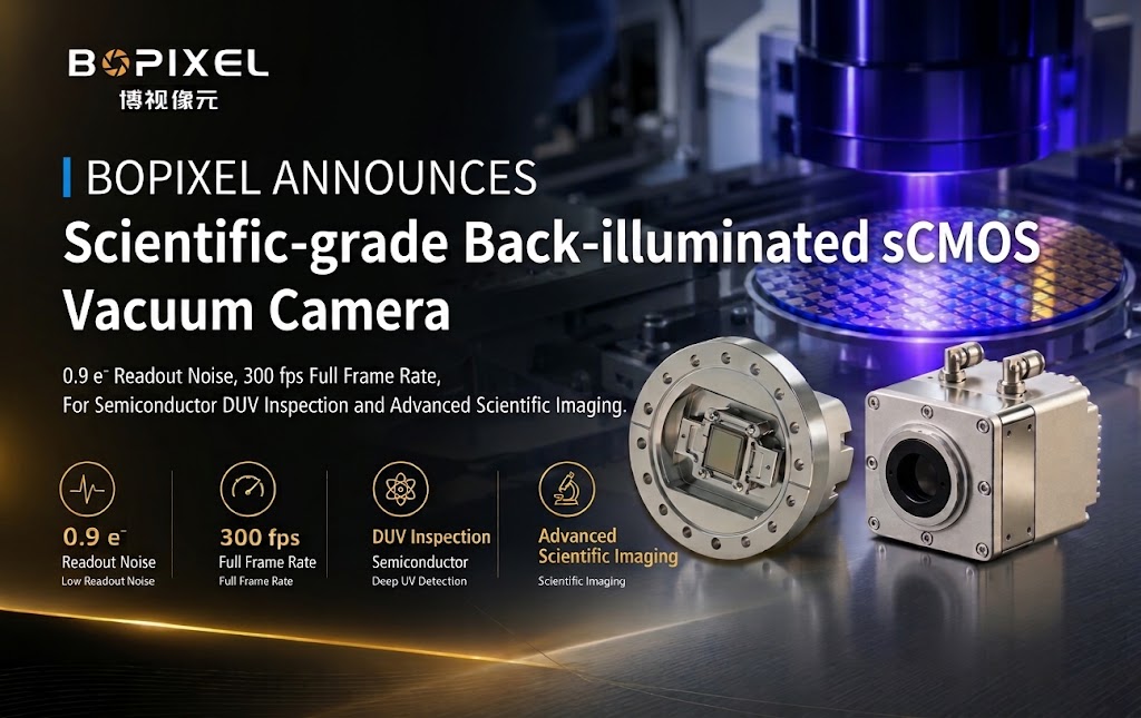
October 27, 2026 —— BOPIXEL announces the release of two scientific-grade sCMOS cameras: the BC-GM4MU3V10 and the BC-GM4MU3V10-VAC. Built upon the Gpixel GSENSE6504BSI back-illuminated scientific CMOS sensor, the new cameras feature a 4.2-megapixel resolution (2048 × 2048) with a 6.5 μm pixel size. They achieve a read noise of 0.9 e⁻ (rms), a dark current of 0.004 e⁻/pixel/s at a sensor temperature of -30°C, and full-resolution frame rates of up to 300 fps. The VAC model features a CF100 vacuum flange, allowing direct mounting into vacuum chambers or spectrometers. It is designed for deep ultraviolet (DUV) semiconductor inspection and metrology, low-light spectroscopy, neuroscience, and live-cell imaging.
I. Shorter Wavelengths, Weaker Signals: Noise Becomes the System Limit
Front-end semiconductor inspection is tightening along two fronts: defect sizes are shrinking alongside process nodes, pushing inspection wavelengths into the deep ultraviolet spectrum. However, DUV light source power, optical transmittance, and material absorption depress the photon count reaching the sensor to single- or double-digit levels. Under these conditions, read noise can no longer be ignored—it directly determines whether a defect is "detectable" or "undetectable." Similarly, dark current in long-exposure metrology raises the background floor and compresses dynamic range. Single-molecule fluorescence, super-resolution, and in vivo neural imaging face the exact same constraints: signals are counted in individual photons, exposures extend from milliseconds to tens of seconds, and dark current accumulates fully over time.
II. Three Core Capabilities Pushing Detection Limits to Single-Photon Levels
- Sub-Electron Read Noise: A read noise of 0.9 e⁻ (rms) enables single-photon charge packets to be distinguished from the noise floor. Ultra-weak signals no longer require extended integration times or intense illumination to maintain signal-to-noise ratio (SNR), boosting defect detection rates under identical light source power or easing light source heat loads and degradation.
- Deep Cooling & Low Dark Current: TEC water cooling lowers sensor temperature to -30°C, holding dark current down to 0.004 e⁻/pixel/s. A 60-second exposure accumulates only ~0.24 e⁻ of dark charge per pixel, making long exposures a practical and viable tool.
- Hermetic Vacuum Sealing: Combining vacuum encapsulation with TEC water cooling prevents condensation, contamination, and cooling efficiency decay. It eliminates calibration drift caused by repeated defrosting or thermal fluctuations, making it ideal for production equipment running continuously for weeks or multi-day live-cell experiments.
III. Broadband Sensitivity: From DUV to NIR
The back-illuminated architecture delivers a peak quantum efficiency (QE) of 95% at 450 nm and maintains an average QE above 50% across 200–300 nm, providing a broadband spectral response spanning 200–1100 nm. The dual-gain HDR mode achieves a dynamic range of 83.4 dB, capturing bright scattering backgrounds and faint defects in a single frame, eliminating multi-exposure fusion overhead and registration errors. The USB 3.2 Gen2x2 interface is GenICam-compliant and supports free-run, external, and Link triggering modes for seamless integration into existing motion stages, light sources, and acquisition software.
IV. Two Form Factors & Typical Applications
The standard model caters to conventional optical systems, while the VAC model mounts directly onto vacuum chambers or spectrometers via its CF100 flange, eliminating window transmission losses and alignment errors. Both models share the same imaging core and software interface, simplifying platform-level integration for OEMs.
Key Applications Include:
- Semiconductor Inspection & Metrology: DUV brightfield/darkfield defect inspection, mask and wafer surface review, weak-signal imaging in critical dimension (CD) and overlay metrology, as well as SiC and GaN substrate and epitaxial la yer defect characterization.
- Spectroscopy: Raman, fluorescence, and plasma emission spectroscopy (OES), plus in situ monitoring of vacuum deposition and etching processes.
- Life Sciences: Single-molecule imaging, super-resolution microscopy, light-sheet microscopy, long-term live-cell imaging, and in vivo calcium imaging.
- Physics & Advanced Optics: Quantum optics single-photon detection and adaptive optics wavefront sensing.
V. Availability
Both models are available for order immediately. BOPIXEL provides evaluation units, SDKs, and integration support, along with customizable optical interfaces, cooling solutions, and vacuum configurations.
VI. About BOPIXEL
BOPIXEL focuses on scientific-grade and industrial-grade imaging products, including scientific sCMOS cameras, vacuum cameras, and high-speed imaging systems. The company serves equipment OEMs and research institutions across semiconductor inspection, life sciences, and spectral analysis.

- CONTACT INFORMATION
-
Address: 6 / F, Jingdong Technology Building, 76 Zhichun Road, Haidian District, Beijing / 2nd Floor, Building 7, Fengchuang Technology Park, Keji 13th Street Beijing Economic-Technological Development Area, Beijing
Telephone: +86 010-64754979
- Sales Consulting
-
E-Mail:
overseas@bopixel.com
Telephone: +86 13311070920 Ms.Tracy Dai
- Technical Support
- E-Mail: support@bopixel.com
- PRODUCTS
- Structured Light 3D Camera
- High Speed Area Scan Camera
- HIGH SPEED LINE SCAN CAMERA
- DLP Projector
- Cr Series Code Reader & Industrial Smart Camera
- Ultra-high speed camera
- Line Laser 3D Profiler
- Frame Grabber






© 2023 Copyright Beijing BOPIXEL Technology Co., Ltd.Beijing Icp No. 2022013801